Check the open call for Ph.D. positions (deadline March 15)
12 new Ph.D. scholarships now available (39° cycle)
Read more
PNRR establishes doctoral programmes in the areas of Key Enabling Technologies
466 co-financed Ph.D. scholarships at PoliMi for industrial partnerships
Read more
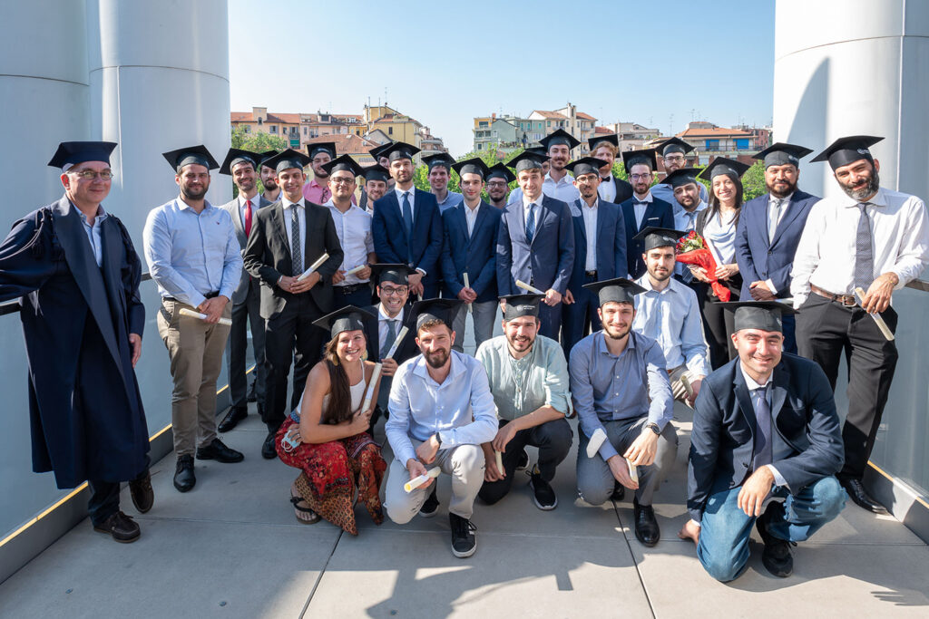
On May 19, 2023, a graduation ceremony was held to confer the doctoral degrees to the 62 students of the Ph.D. course in IT
Ceremony of Conferral of Doctoral Degrees 2023
Read more
Take the survey and let us know your thoughts about the new Ph.D. IT website!
Ph.D. IT Website Survey
Read moreLatest news and events
No available posts.
Colloquia Doctoralia
Keynote & award speeches


Explore the Ph.D. IT programme
Get here all the information about the the Ph.D. programme in Information Technology of the Politecnico di Milano
Ph.D. stories
Our community
The DEIB Community is the digital community of the Dipartimento di Elettronica, Informazione e Bioingegneria of the Politecnico di Milano. The project was developed to enhance experiences and skills, aggregate talents and generate innovation through cooperation, continuous exchange and goal sharing between academic research and the industry world.
What are our Ph.D.’s doing now?
Industrial partners
Check out some of our recent sponsors of Ph.D. scholarships.
STMICROELECTRONICS
LEONARDO SPA
LUXOTTICA SRL
TIM S.P.A.
SILK FAW AUTOMOTIVE GROUP S.R.L.
CONTENTWISE S.R.L.
FONDAZIONE TELETHON ETS
HUAWEI TECHNOLOGIES ITALIA SRL
ODYS SRL
RICERCA SISTEMA ENERGETICO – RSE S.P.A.
TRE ALTAMIRA SRL
A2A S.P.A.
ADIGE S.P.A
ANTARES VISION S.P.A.
ATLANTE SRL
BRAVONEXT SA
CEA-LETI
CNR-STIIMA
DHIRIA S.R.L.
E4 COMPUTER ENGINEERING SPA
Evidence S.R.L.
FONDAZIONE CARIPLO – XNEXT
FONDAZIONE POLITECNICO DI MILANO
Free2move eSolutions S.p.A.
GoQuantum
HITACHI ENERGY ITALY S.P.A
IIT – ISTITUTO ITALIANO DI TECNOLOGIA
INVENTVM
ISTITUTO DI RICERCHE FARMACOLOGICHE MARIO NEGRI IRCCS
KNOBS SRL
LUCCHINI RS SPA
MBDA ITALIA SPA
MOVYON S.P.A.
NEC LABORATORIES EUROPE GMBH
NUOVO PIGNONE SRL
PIRELLI TYRE S.P.A.
SIEMENS
SPEEDY SRL
SUPSI
THALES ALENIA SPACE ITALIA
TRUESENSE S.R.L.
VICOMTECH